

![]()
![]()
![]()
![]()
![]()
MicroCap is usually considered to be restricted to low frequency linear (e.g. audio) and non linear (switch-mode power supply) simulation. Consequently it's in built models tend to ignore RF related device parameters.
This obstacle is surmountable however. MicroCap is quite capable of performing adequate RF simulation if it is used with a small amount of imagination. Obviously, a dedicated RF simulation platform (ADS, Eagleware etc) is preferable, but the financial cost of these simulation tools is well beyond the financial reach of most amateur scientists and electronic hobbyists.
I will demonstrate MicroCap's RF capability in this web chapter using an HF Voltage Controlled Oscillator (VCO) as an example. This design is intended for a QRP amateur radio transceiver intended to operate in the 80 meter frequency band (3.5 MHz to 3.9 MHz) i.e. 80 meter transceiver
I decided on a simple "Colpitts" circuit topology using a BC559 PNP bipolar transistor using model parameters that I extracted using the procedure I discussed in the previous web chapter NPN_model . I used a BB212 / MVAM108 "hyper abrupt" varicap diode model for this application due to its high capacitance and capacitance range combined with a relatively low tuning voltage range (Cd{0.5 V} = 600 pF, Cd{8.0 V} = 15 pF)

Notes:
This VCO can be referred to as a negative resistance oscillator, at least for the purpose of analysis. The transistor provides Transconductance Gm that combines with the reactance of C2 and C4 to produce a negative resistance term in series with a capacitive reactance Zb (at the base terminal). This complex impedance is in series with the reactance of coupling capacitor C3 resulting in a total source impedance Zbb given by
Zbb = - Rs - j · Xs
where Rs = Gm · X2 · X4
and Xs = X2 + X3 + X4
with Xk = 1 / [ 2 · pi · FRF · Ck ] ; k = 2, 3, 4
The source impedance is presented to the "resonant load" comprised of L1 ,C1 ,C6 and C{D1} in parallel form, i.e. as an admittance i.e.
Ybb = 1 / Zbb
Ybb = - Rs / [ Rs2 + Xs2 ] + j · Xs / [ Rs2 + Xs2 ]
It is however sometimes preferred to consider the admittance Y = G + j B in reciprocal form i.e. Y = [ 1 / Rp ] + j · [ 1 / Xp ] (i.e. as two parallel terms). In this case we have
Rp = - [ Rs2 + Xs2 ] / Rs
Xp = - [ Rs2 + Xs2 ] / Xs
Alternatively we can rewrite these equations as
Rp = - Rs · [ 1 + Qs2 ]
Xp = - Xs · [ 1 + Qs-2 ]
where Qs = Xs / Rs = [ X2 + X3 + X4 ] / [ Gm · X2 · X4 ]
The Transconductance Gm for an ideal bipolar transistor at room temperature is proportional to its collector current and can be estimated from
Gm = 0.04 · Ic Amps/Volt
where the collector current is in mA. The circuit shown biases the base of the PNP transistor at "half rail" i.e. 4 Volts given that the supply voltage was set to Vcc = 8 Volts. Sine the emitter voltage is 0.7 Volts higher, the voltage drop across R5 will equal 3.3 Volts corresponding to an emitter current of Ie = 3.3 mA. Since the base current Ib is comparatively small (HFE > 300 for the BC559 transistor) the collector current Ic will also (approximately) equal Ie . This implies that the transistor Transconductance will approximate Gm ~ 0.13 A/V
Predictions:
Let us consider VCO operation at its center frequency of FRF = 3.7 MHz with Gm = 0.13, C2 = C4 = 470 pF and C3 = 47 pF. This implies
Gm = 0.13 Amps/Volt
X2 = X4 = 92 Ohms
X3 = 920 Ohms
Rs = 1,100 Ohms
Xs = 1,104 Ohms
Qs = 1.004
Rp = 2,208 Ohms
Xp = 2,200 Ohms
Cp = 20 pF
Of these terms the "effective parallel capacitance" Cp should be treated with some caution as it is Gm dependent and equals 1 / [ 1 / C2 + 1 / C3 + 1 / C4 ] when Gm = 0. At "start up" the Transconductance Gm will be higher than when the oscillator has reached a "steady state amplitude". The actual steady state value of Cp will increase and become closer to the series combination of C2 , C3 and C4 .
For oscillations to start, the total parallel resistance at node "V_TC" must be negative. This requires that Rp < Rp, L1. Since L1 = 3.3 µH we have XL1 = 77 Ohms, defining a component Q of about 100. This implies an equivalent parallel resistance of 7.7 kOhm (same Q).
The active source negative parallel resistance was equal to 2.2 kOhm, i.e. I have set an excess ratio of 3.5 : 1 to ensure reliable oscillation start-up
MicroCap (student) provides Fast Fourier Transform (FFT) analysis of time domain waveforms allowing spectrum analysis. This feature is very effective for "continuous" time domain waveforms but the dynamic amplitude range of any FFT is compromised when the input time domain waveform has discontinuities. This difficulty is especially apparent when oscillators are analyzed for spectral purity. It takes a finite time for oscillations to build up in an oscillator and this discontinuity causes an extreme elevation of the FFT "noise floor" in addition to close spectral spreading.
The standard approach to this problem is to "window" the time domain data with a window function that forces the start and end portions of a captured time domain signal signature to be the same. This is equivalent to interpreting this time domain waveform to be of infinite length since the truncated segment can be concatenated (placed end on end) as identical replicas with no loss or addition of information.
I include a simple cosine window in the VCO circuit file. This starts at 0 and peaks at a value of 2 then falls back to a value of zero. This is multiplied by the input time domain waveform to force it as appearing to repeat indefinitely.
The window time length was set to T = 1 ms, the simulation time was set to T = 2 ms and therefore 2 "windows" are applied to the simulation waveform. The second window from T = 1 ms to T = 2 ms is used for FFT analysis as by this time the VCO waveform has accurately settled to steady state.
The windowed FFT enhances the amplitude dynamic range for signals that are not exactly periodic, as will usually be the case with uncontrolled oscillator waveforms. Some spectral spreading will still occur but usually the overall spectral result will be better than having no window function at all.
I also included a 50 Ohm load on the voltage input to this FFT analysis "front end" to emulate a real spectrum analyzer, and a scaling factor to allow the subsequent FFT to read spectral power directly in dBm, also in accordance with conventional spectrum analyzer scaling.
The circuit file shows the use of a Non Linear Transform to correct the inaccuracy of the standard varicap capacitance versus reverse bias voltage model. I have expanded this approach in the following web chapter (MATHCAD)
Varicap diodes have improved greatly over time but unfortunately the "standard model" no longer applies to them due to excessive inaccuracy. This MATHCAD section will show how to resolve this obstacle and so explain the use of a Non Linear transform shown in the previous circuit file

The VCO circuit "transient" simulation was run for a time length of T = 2 ms with a minimum time step equal to 2 ns. This results in a simulation time of about 1 minute. Although this may seem excessive, it should be considered with the following comparisons
| The time required to build and test an actual VCO would be a lot longer than 1 minute! | |
| The equipment cost required for testing would far exceed the cost of MicroCap student version as this is free! | |
| The minimum time step can be increased and the simulation time reduces favorably at the expense of amplitude resolution |
So, in summary this RF application "stretches" MicroCap's capability far beyond its original intentions but it holds up well to the challenge!
Now to consider the time domain waveforms generated from the transient analysis option in MicroCap
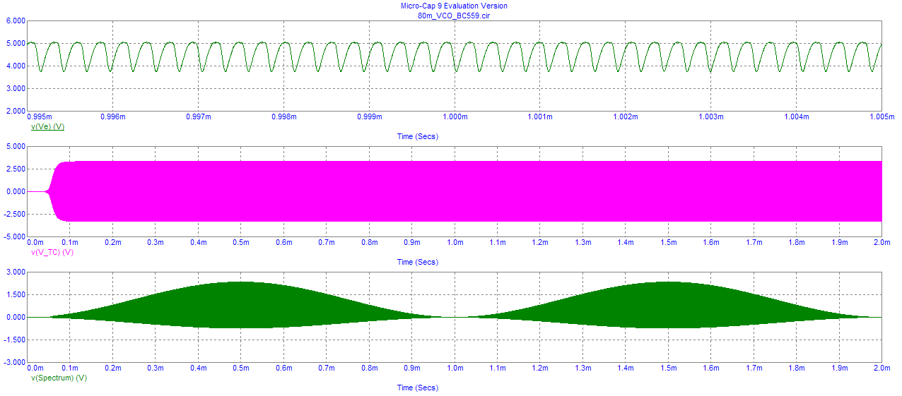
We observe the emitter voltage on the top trace, oscillating between 3.9 V and 5.0 V and with a pseudo sinusoidal shape (i.e. has harmonics). The time axis has been expanded to look close in and it appears that about 3 1/2 cycles fit within each 1 µs interval, i.e. the oscillation frequency is about 3.5 MHz.
The second waveform shows the complete time domain trace. Notice the oscillator start up time is about 800 us or so to reach maximum amplitude. This waveform was measured at the top of the resonant tuned circuit i.e. V_TC. The peak RF voltage appears to be about 3 Vpeak .
The lower waveform shows the windowed time domain waveform obtained from the collector of Q1 . The second window was used for subsequent FFT analysis.
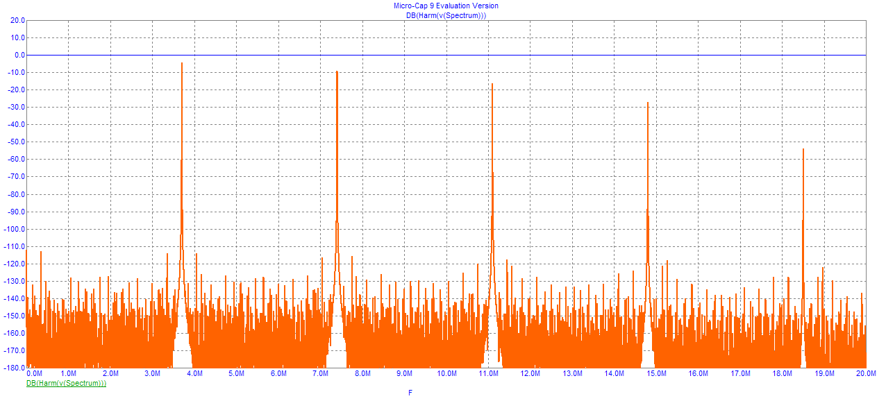
This display shows the FFT applied to this second time domain waveform window (TMAX, TMAX/2). The fundamental frequency is about 3.7 MHz from this display with a power amplitude about -4 dBm. The 2, 3 and 4 harmonic terms can be seen. The FFT noise floor has some spikes caused by finite numerical resolution, but these as extremely low. The worst spur is about -112 dBm suggesting an amplitude dynamic range close to 110 dB ! This range is extremely good and few real world spectrum analyzers could achieve this level of performance.
Also it is instructive to note that the second time window was 1 ms in length corresponding to a resolution bandwidth BW = 1 / 0.001 = 1 kHz. A conventional "swept" spectrum analyzer would need to tune to 20 MHz / 1 kHz = 20,000 "channels" in comparison. Let's assume each "channel" requires at least 1 ms of time to "settle" to a measured value. The corresponding sweep time would therefore be at least 20 seconds. Again, MicroCap performed no worse in this regard!
Now let's look closer in at the VCO phase noise performance (Øn ). Physical measurement for phase noise is specialized and expensive. I have used MicroCap to demonstrate some very credible capability in this area. The previous circuit file VCO appears to have a phase noise performance equal to Øn = 140 dB1000 Hz at a frequency offset of 100 kHz when measured in a FFT bandwidth of 1 kHz. This corresponds to a phase noise ratio of Øn = 170 dB1 Hz at this offset.

This plot was simulated with a varicap control line voltage equal to V_Tune = 4.0 V. The intended frequency range for this VCO was 3.5 MHz to 3.9 MHz using a varicap control voltage of V_Tune = 0.5 V to V_Tune = 7.5 V. The center frequency has been set mid range with V_Tune also set mid range. Now lets look at the lower frequency tuning extreme, i.e. V_Tune = 0.5 V
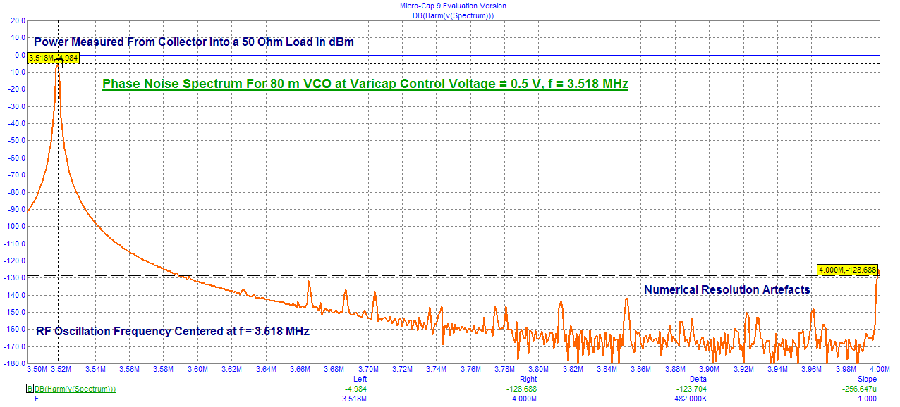
We note the new VCO frequency has fallen to FRF = 3.518 MHz. This is very encouraging and surprisingly linear! Now lets simulate the VCO at V_Tune = 7.5 V
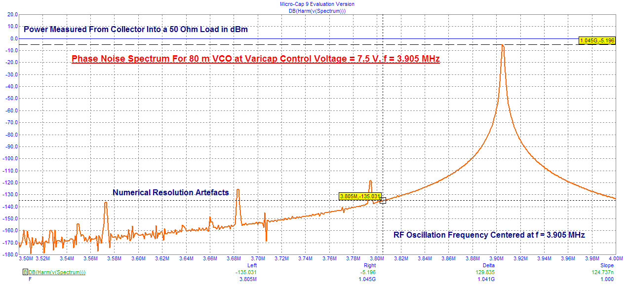
This time the VCO carrier frequency has increased to just over 3.9 MHz. This result is also very encouraging and suggests linear tuning has been achieved!
This Web Chapter has shown MicroCap (student) used far beyond its typical expectations and has shown very credible prediction accuracy for a reasonable VCO intended for RF operation at 3.7 MHz.
MicroCap has shown RF time domain waveforms, start up oscillation time, output power in dBm, harmonic power in dBm up to 20 MHz, an amplitude dynamic range exceeding 110 dB and an ability to measure close in phase noise Øn down to Øn = 170 dB1 Hz @ 100 kHz offset.
In addition, the inaccurate "standard model" for varicap diodes was shown to be pitiful when applied to real hyper abrupt varicap diode capacitance data. The BB212 / MVAM108 varicap was used as an example in a MATHCAD file. However I have proposed a simple solution based on applying a exponential conversion between control line voltage and the voltage passed on the varicap model (standard) used in MicroCap. This resulted in exceptional predictive capacitance versus reverse bias accuracy and this benefit then allowed the tuning range of the VCO to be simulated with favorable outcomes (i.e. linear tuning at 3 points)
Consequently we see that MicroCap's simulation functionality can be extended into RF analysis with a bit of imagination, and result is very useful predictive outputs.
I intend to add further to this "campaign" and the next web chapter will show MicroCap used to measure two tone intermodulation performance of a medium power RF amplifier intended for Single Sideband (SSB) operation at 3.7 MHz! Once again, MicroCap will be used to its full extent of capability.
![]()
Return to Microcap Simulation
or Ian Scotts Technology Pages
© Ian R Scott 2007 - 2008